ARM LPC2138/48 Mini Development Board – Overview
LPC2138/48 mini development board from rhydolabz is an easy to handle, general purpose development board built around LPC2138/48 (microcontroller based on ARM7TDMI-S CPU) and related peripherals. The board is designed with a variety of hardware to exercise LPC2138/48 microcontroller peripherals. Mini Bread board is also provided to ease the use. Ideally suitable for training and development purposes.


Key Features![]()
- Compact design and user friendly
- LPC2148 MCU is integrated onto the board
- No separate Programmer required (Built in Bootloader)
- On-board 12 MHz crystal for controller
- Multiple power input options (USB, RMC Connector, DC barrel jack) with jumper selection
- Reverse supply voltage polarity protection
- On-board 5V and 3.3V regulators
- 3.3 and 5V output available on berg strip
- Power indication LED (Red)
- Servo, LCD & ZigBee can be easily interfaced through on-board connectors
- ZigBee communication through UART0
- Provision for ZigBee connectors on either side of the board
- Potentiometer for LCD contrast control
- On-board buzzer
- 4 on-board switches including a reset switch & 3 others connected to port pins via jumpers
- 3 on-board SMD LED s connected to port pins via jumpers
- Potentiometer connected to ADC via jumper
- Temperature sensor (MCP 9700) connected to ADC via jumper
- On Board ICD Connector for Debugging
- All port pins are accessible through both male & female berg strips.
- UART0 communication possible through ZigBee, DB9 connector,USB and RMC connector
- UART0 on can be used in 3.3V and 5V levels(with jumper selection) through RMC connector
- UART1 communication possible through berg strip connector
- Internal USB of LPC2148 is accessible through on-board USB port
- Breadboard can be attached to the board
- 32.768 kHz crystal for internal RTC
- Battery holder for external battery used to power RTC
- Multiple programming options – USB, Serial port
- Programmer switch to select 2 programming modes :
i. Auto – no reset, no ISP jumper
ii. Manual – Press reset switch, use ISP jumper - ISP jumper should be removed for code execution
- For UART0 communication, programmer switch should be in manual mode
- Professional EMI/RFI Complaint PCB Layout Design for Noise Reduction
- High quality two layer PTH PCB
LPC 2138 Specifications![]()
- High Performance 32-bit ARM7TDMI-S™ CPU
- 512 KB Programmable Flash Memory provides minimum of 10,000 erase/write cycles and 10 years of data-retention.
- 32 KB Data Memory (SRAM)
- In-System/In-Application Programming (ISP/IAP) via on-chip boot-loader software.
- Single Flash sector or full chip erase in 400 ms and 256 bytes programming in 1 ms.
- EmbeddedICE and Embedded Trace interfaces offer real-time debugging with the on-chip RealMonitor™ software and high speed tracing of instruction execution.
- Two 8-channel 10-bit A/D with conversion times as low as 2.44 us per channel.
- Single 10-bit D/A converter provide variable analog output.
- Two 32-bit Timers/External event counters.
- Four Capture and four Compare channels.
- PWM unit with six output pins.
- Low power Real-time clock with independent power and dedicated 32 kHz clock input.
- Multiple serial interfaces including two UARTs, two Fast I2C (400 kbit/s), SPI™ and SSP with buffering and variable data length capabilities.
- Vectored interrupt controller with configurable priorities and vector addresses.
- Up to 47 of 5 V tolerant general purpose I/O pins.
- Up to nine edge or level sensitive external interrupt pins.
- 60 MHz maximum CPU clock available from programmable on-chip Phase-Locked Loop (PLL) with settling time of 100us.
- On-chip integrated oscillator operates with external crystal in range of 1 MHz to 30 MHz or with external oscillator from 1 MHz to 50 MHz.
- Power saving modes include Idle and Power-down.
- Individual enable/disable of peripheral functions.
- Processor wake-up from Power-down mode via external interrupt or Real-time Clock.
- Single power supply chip with Power-On Reset (POR) and Brown-Out Detection (BOD)
- CPU Operating Voltage range of 3.0 V to 3.6 V
LPC 2148 Specifications![]()
- High Performance 32-bit ARM7TDMI-S™ CPU
- 512 kB Programmable Flash Memory provides minimum of 10,000 erase/write cycles and 10 years of data-retention
- 32 kB + 8 kB Data Memory (SRAM)
- Provides 8 kB of on-chip RAM accessible to USB by DMA
- Two 10-bit ADCs provide a total of 14 analog inputs, with conversion times as low as 2.44 us per channel
- Single 10-bit DAC provides variable analog output
- Two 32-bit Timers/External event counters
- Four Capture and four Compare channels
- PWM unit with six output pins
- Low power Real-time clock with independent power and dedicated 32 kHz clock input
- Multiple serial interfaces including two UARTs (UART0 & UART1), two Fast I2C (400 kbit/s), SPI™ and SSP with buffering and variable data length capabilities
- Vectored interrupt controller with configurable priorities and vector addresses
- Up to 45 of 5 V tolerant general purpose I/O pins
- Port pins P1.0-P1.15 & P0.24 are not externally accessible. P0.31 is output only digital pin. P0.26 & P0.27 cannot be used as GPIO pins since these are dedicated to USB (D+ & D- respectively)
- Up to nine edge or level sensitive external interrupt pins
- USB 2.0 Full-speed compliant device controller with 2 KB of endpoint RAM
- In-System Programming/In-Application Programming (ISP/IAP) via on-chip boot loader software
- Single Flash sector or full chip erase in 400 ms and programming of 256 bytes in 1 ms
- Embedded ICE RT and Embedded Trace interfaces offer real-time debugging with the on-chip Real Monitor software and high-speed tracing of instruction execution
The following figures illustrate the peripheral features of the board
- J7,J9 – To select serial port/USB port for UART0 communication
- SW5(Programmer switch) – To select auto/manual mode of programming
- J15(ISP jumper) – To be shorted in manual mode of programming & should be removed for code execution
- Power LED – Glows when the board is powered
- K2(Power jumper) – To select power source as USB/DC source
- J8 – To enable 20 pin JTAG connector for debugging
- LED – On-board SMD LED s
- SWITCH – On-board switches
- SW4 – Reset switch

- J11 – Connects temperature sensor to P0.28(AD0.1)
- J12 – Connects potentiometer to P0.29(AD0.2)
- J1,J2,J3 – Jumpers connecting LED s to port pins P0.17, P0.18 & P0.19
- J4,J5,J6 – Jumpers connecting switches to port pins P0.14, P0.15 & P0.16
- J10 – Jumper connecting buzzer to port pin P0.21
- K14 – Connector to access UART0
- K13 – Connector to interface servo
- J16 – Jumper to select 3.3/5 V level when using UART0 through K14
- K12 – Connector to access UART1
- LCD – Berg strip connector for LCD
Layout![]()
 Powering
![]()
The board can be powered in 3 ways
- USB connector
- DC Barrel Jack
- RMC Connector
The input source can be selected as DC/USB using the jumper. If DC source is selected, then either DC Barrel Jack or RMC connector can be used and the supply voltage should be in the range of 7-12 V.Once the board is powered, the power LED(red LED on the board) glows.
How to test?![]()
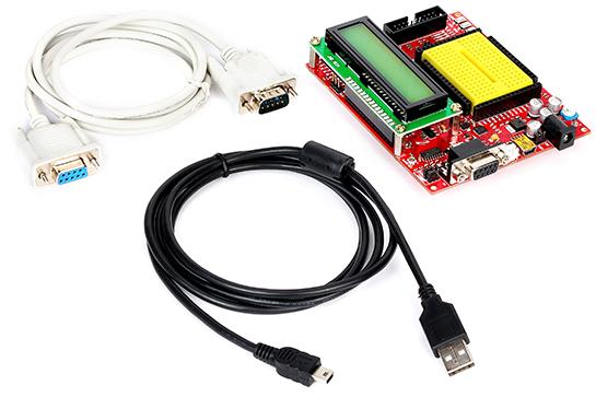
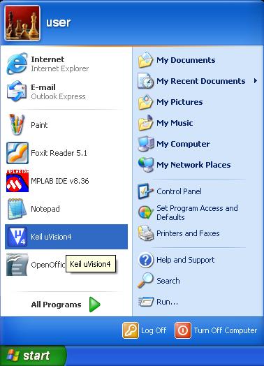
The code for LPC 2138/48 is written in Keil uVision4 IDE(Download). Various steps are explained below.
- Step 1: Launch Keil uVision4
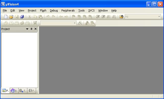
- Step 2: The Keil uvision window opens as shown below
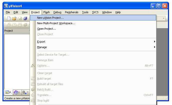
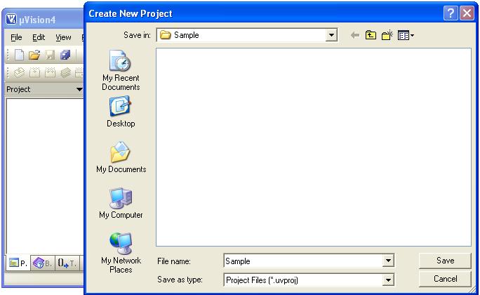
- Step 3: To create a new project, select Project > New uVision Project from menu bar
- Step 4: Save the project in a suitable location with appropriate name
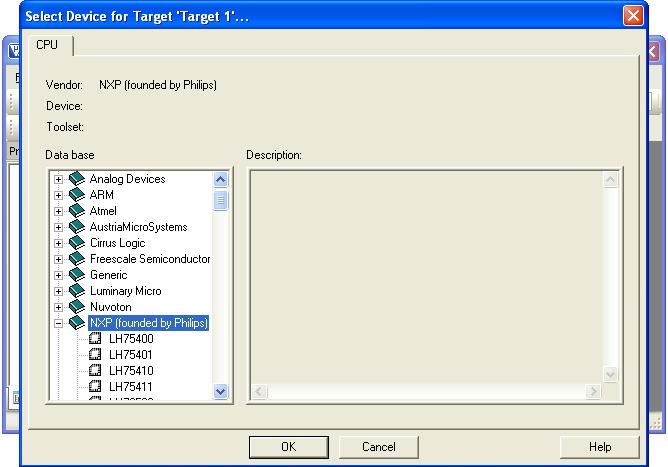
- Step 5: The following window opens. Select (LPC2138) , (LPC2148) (listed under NXP) from the drop-down list
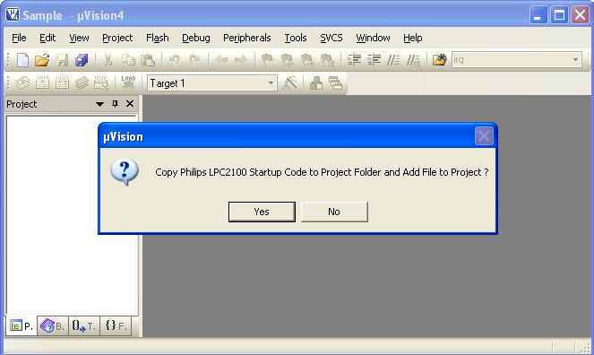
- Step 6: Click ‘Yes’ for the following question to copy the Startup code to Project folder and add file to project
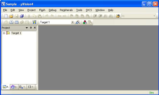
- Step 7: This creates a target to the project
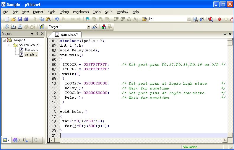
- Step 8: Create a new file either by clicking the New File icon, or by selecting File > New or using keyboard shortcut CTRL + N
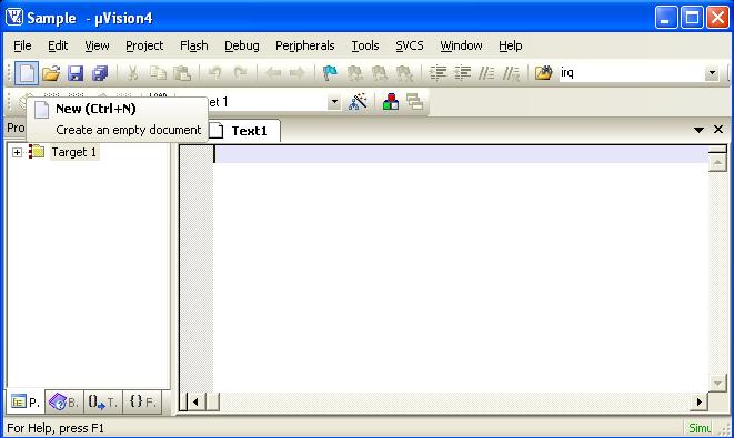
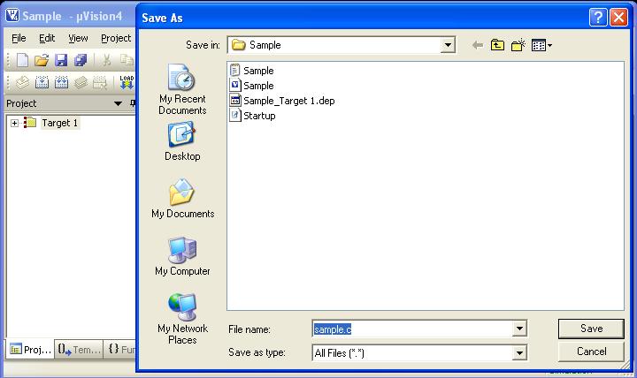
- Step 9: Save the file with .c extension in the project folder
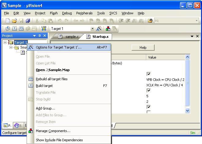
- Step 10: Double click on “Startup.s” to open the configuration window
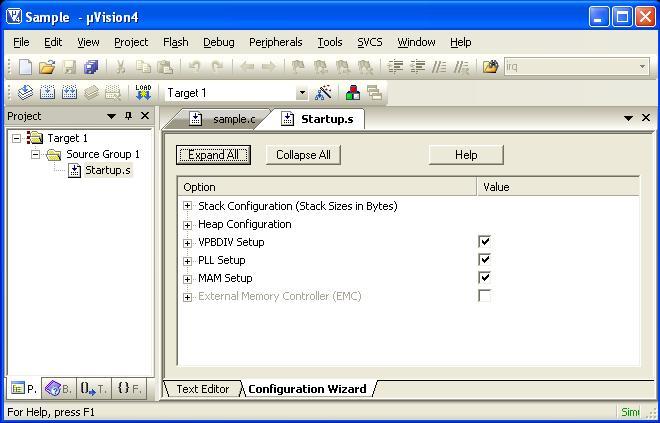
- Step 11: Set the options as shown below and save
The PLL setup is done for 12MHz crystal. The divider (P) and multiplier (M) are selected such that the PLL output is 60MHz and and frequency of PLL current controlled oscillator is within the specified range of 156 – 320 MHz. If crystal frequency is changed, then these values must be changed accordingly.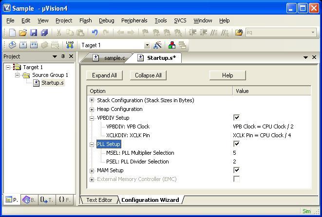
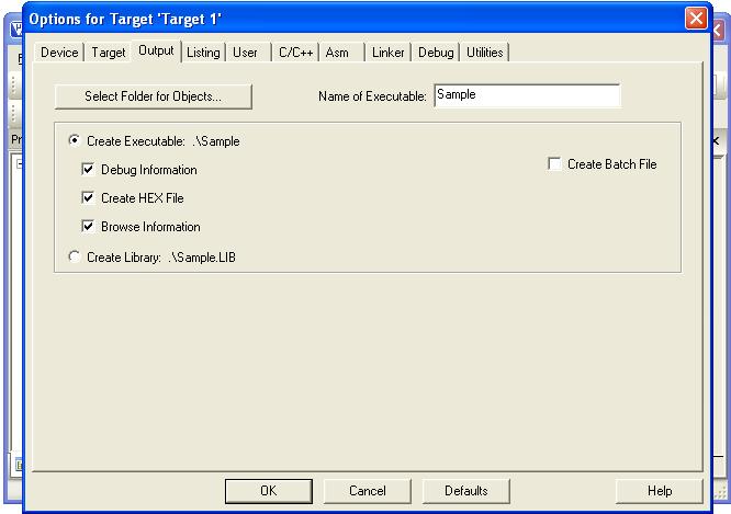
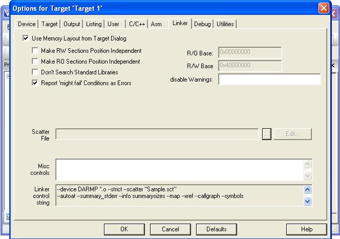
- Step 12: Right click on Target1 to set target file options. You can also do this by using the icon on ‘Build toolbar’ or Project > Options for Target ‘Target 1’
- Step 13: Configure Target, Output and Linker options as shown below
Target – LPC2138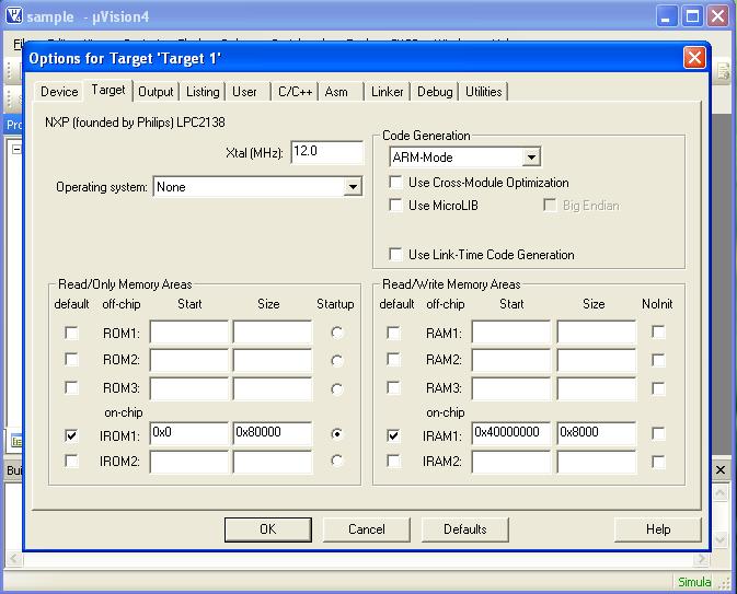 Target – LPC2148
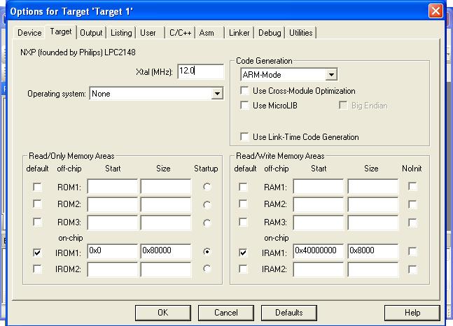 Output
Linker
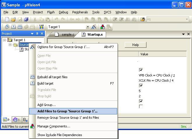
- Step 14: Right click Source Group 1 to add C file to source group
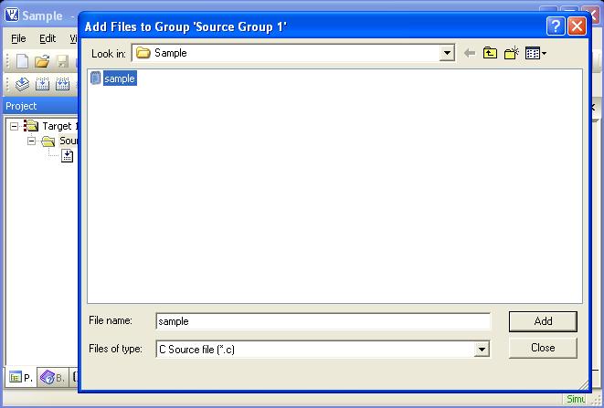
- Step 15: Select the C file created and cilck Add
- Step 16: Now the c file gets added to the Source
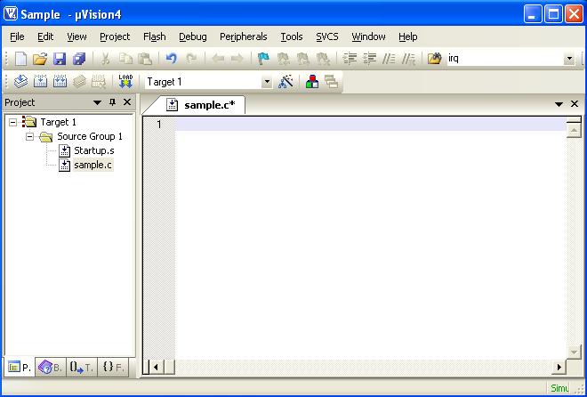
- Step 17: Type the code
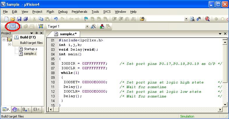
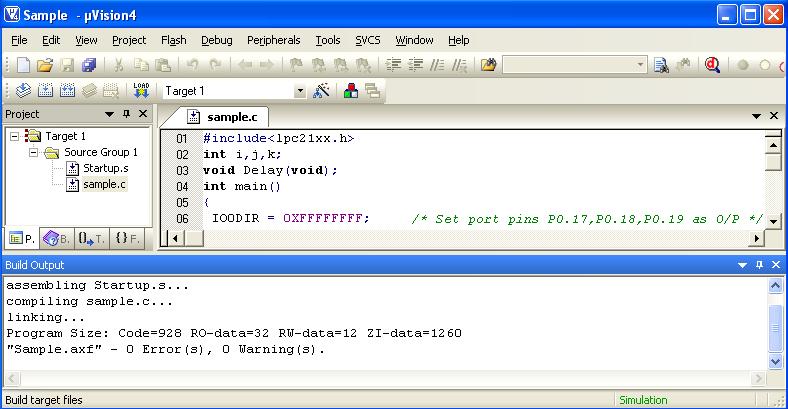
- Step 18: Click the build icon (encircled in figure) to build the project. Errors (if any) get listed in the Build output window. Correct them and build again. On successful building, the hex file will be generated in the project folder
- Step 19: Now the code can be flashed to the controller, follow the same steps for LPC2138/LPC2148.
In the board, do the following jumper connections
- Select the power source as USB cable or DC source
- Select USB or serial port using jumpers J7 & J9 for flashing the code
- Select mode using programmer switch. In manual mode, use ISP jumper. In auto mode, leave it open

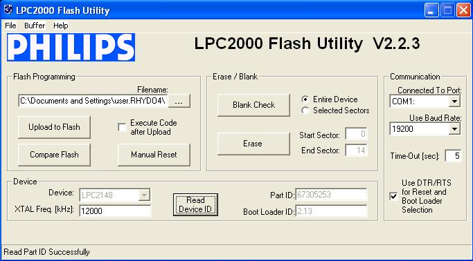
Now power up the board. The power LED(red LED on the board) glows. Open Flash Utility. Select the correct COM port, suitable baud rate and XTAL Freq. 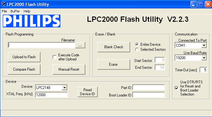
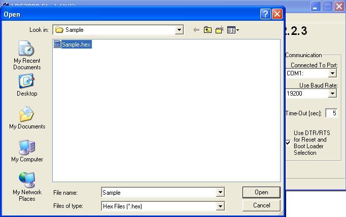
- Step 20: Open the desired hex file
- Step 21: Read device ID
If auto mode is selected, simply clicking the ‘Read device ID’ button will read the ID. But in manual mode, press reset switch and click. When we go for Read Device ID, the ID could be automatically loaded after Read Part ID Successfully .
- Step 22: Click ‘Upload to Flash’
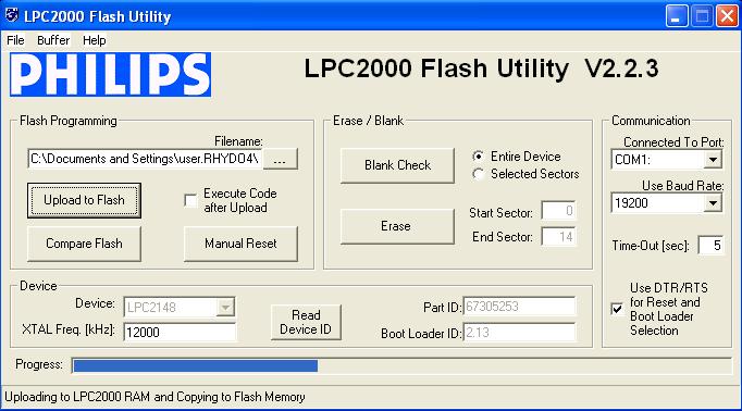
After successfully flashing the code into the controller, remove ISP jumper and reset the board. Also ensure that all the necessary jumpers are shorted. Now the board can be used for the desired purpose.
Topics related to ARM LPC2138/48 Mini Development Board![]()
- ARM LPC2138/48 Mini Development Board – Overview
- ARM LPC2138/48 Mini Development Board – LED Interfacing
- ARM LPC2138/48 Mini Development Board – LCD Interfacing
- ARM LPC2138/48 Mini Development Board – UART0 Interfacing
- ARM LPC2138/48 Mini Development Board – UART1 Interfacing
- ARM LPC2138/48 Mini Development Board – Switches Interfacing
- ARM LPC2138/48 Mini Development Board – BUZZER Interfacing
- ARM LPC2138/48 Mini Development Board – POT Interfacing (ADC)
- ARM LPC2138/48 Mini Development Board – Temperature Sensor Interfacing(ADC)
- ARM LPC2138/48 Mini Development Board – Interfacing Servo motor
- ARM LPC2138/48 Mini Development Board – Internal Real Time Clock (RTC)
- ARM LPC2148 Mini Development Board – USB Interfacing (Human Interface Device)
Resources
![]()
- Softwares
- Datasheets
How to buy?![]()
- Click here to buy rhydoLABZ ARM LPC2129 Development board-Mini
- Click here to buy rhydoLABZ ARM LPC2138 Development Board-Mini
- Click here to buy rhydoLABZ ARM LPC2148 Development Board-Mini
Support![]() Please share your ideas with us, visit our forum for discussion
Please share your ideas with us, visit our forum for discussion