AT89S52 Mini Development Board – Overview
The AT89S52 Development Board Mini from rhydolabz is a general purpose, low cost development board for Intel 8051-compatible family of 8 bit microcontrollers (AT89xxx and P89Vxx manufactured by ATMEL and PHILIPS respectively). It is the new addition to the family of AT89S52 Development kits, featuring a spec level that ranges between the Main Development Boards and the Quick Start Boards from rhydolabz. This mini development board is perfect to start out with 8051 programming and also for designing and testing, simple to highly advanced, 8051 projects.
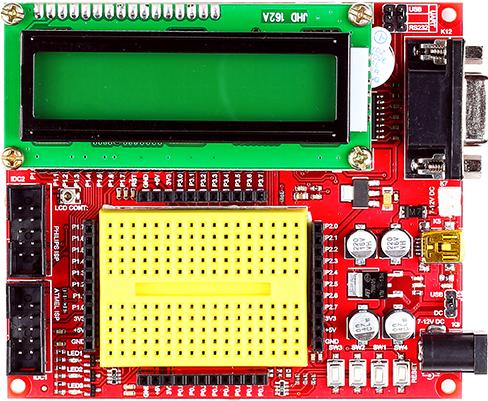
Compatibility![]()
The AT89S52 Development Board (Mini) V1.01 is compatible with the AT89 series of microcontrollers from ATMEL and the P89V series of microcontrollers from PHILIPS. The microcontroller is held on a 40 pin IC base provided on the board. Hence DIP40 package of any microcontroller that belongs in the foretold series (AT89xxx /P89xx) will be apt for use with this development board. The AT89 series remains very popular as general purpose microcontrollers , due to their industry standard instruction set, and low unit cost. This allows a great amount of legacy code to be reused without modification in new applications. AT89S52 Development Board (Mini) V1.01 package as its name suggests includes the ATMEL make AT89S52 microcontroller (DIP40). The following section opens up the specification of the same.
 Key Features
![]()
- Compact and ready to use design
- Two layer High Quality PTH PCB
- Compatible with AT89xxx / P89Vxx controllers
- Includes AT89S52 microcontroller
- ICSP connector ports (5X2 IDC)
- Resistant to voltage variation (7V to 12V DC)
- Power supply reverse polarity protection
- 3 power supply* options (USB/RMC connecter/Wall Wart)
- 5V (1A) and 3.3V (800mA) regulated power output on board
- All port pins available at male berg strip connector pins
- Provision to attach mini breadboard on the board
- Port pins connected* with switches (3x), LEDs (3x) , buzzer
- On board pull-up for PORT0 pins
- On board 11.0592 MHz crystal oscillator
- On board reset switch and power indicator LED
- UART Interface (RS232/USB/3V3/5V)*
- I2C interfaced external EEPROM (24C04)
- On board peripheral support (LCD/ZigBee/RFID/Servo)
AT89S52 Specifications![]()
- 8K Bytes of In-System Reprogrammable Flash Memory
- Fully Static Operation: 0 Hz to 33 MHz
- Three-level Program Memory Lock
- 256 x 8-bit Internal RAM
- 32 Programmable I/O Lines
- Three 16-bit Timer/Counters
- Eight Interrupt Sources
- Programmable Serial Channel
- Low-power Idle and Power-down Modes
- 4.0V to 5.5V Operating Range
- Full Duplex UART Serial Channel
- Interrupt Recovery from Power-down Mode
- Watchdog Timer
- Dual Data Pointer
- Power-off Flag
- Fast Programming Time
- Flexible ISP Programming (Byte and Page Mode)
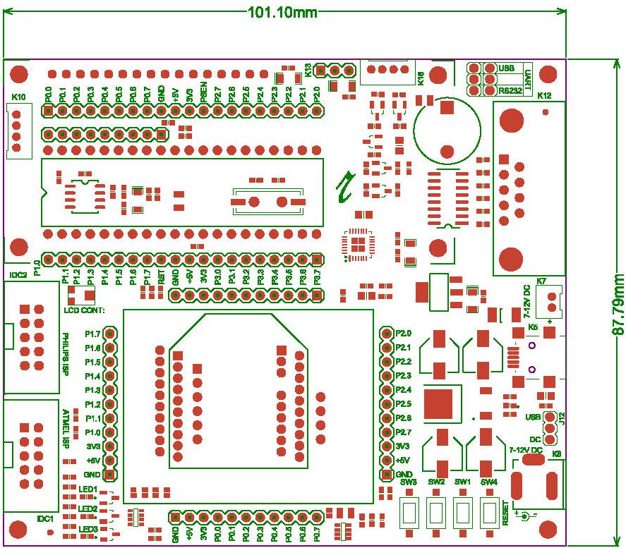
The following figures illustrate the peripheral features of the board:
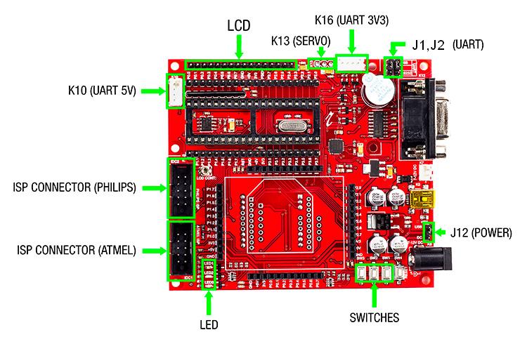
- J1, J2 – To select serial port/USB port for interfacing with PC
- J12 (Power Jumper) – To select power source as USB/DC source
- SWITCH – 3 x On-board switches
- Power LED – Glows when the board is powered
- ISP Connector (ATMEL) – For programming
- ISP Connector (PHILIPS) – For programming
- K10 – Connector for accessing UART(5V)
- LCD – 16 pin Berg strip connector for LCD
- K13 – Connector for interfacing Servo Motor
- K16 – Connector for accessing UART(3V3)
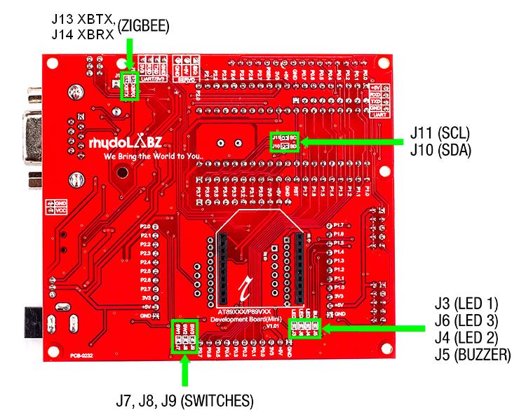
- J13, J14 – Jumper for selecting 3.V3 level at Zigbee RX and TX
- J11, J10 – Connects SCL , SDA to EEPROM (24C04)
- J3, J6, J4 – Jumpers connects LEDs to port pins
- J7, J8, J9 – Jumpers connects Switches to port pins
Layout![]()
 Powering Up
![]() The AT89S52 Development Board (Mini) V1.01 comes with three options of input power supply. It can be powered via either of the following (jumper selectable)
The AT89S52 Development Board (Mini) V1.01 comes with three options of input power supply. It can be powered via either of the following (jumper selectable)
- USB Programming cable (+5V) connected to on board USB connector
- DC adapter (7V – 12V) connected to the on board DC barrel jack
- External DC power supply connected to on board RMC connector
Of the above three input options, the suitable one is selected using on board jumper. The USB/DC powering is selected using the power selection jumper J12. When the board is USB powered it survives slight supply variations (if any) with a help of a fuse provided on the board. If it is powered using an external DC source either via DC barrel jack or the RMC connector, then the board is capable to withstand a voltage variation of 7 to 12 volts. Upon powering up, the blue power indication LED provided on the board will glow. Output pins, are provided on the board with 5V and 3.3V out, which will be very helpful while testing circuits on bread board as well as to power up other external modules.
How to Test ?![]()
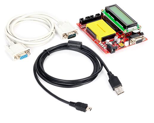
Mini USB (only for powering) and serial cable is used to interfacing with PC. When USB cable is connected to the AT89S52 Mni Development Board, “PWR LED” (Blue) on the top of AT89S52 Mni Development Board glows, which shows the power indication. Follow the steps below to get started with programming your AT89S52 using the rhydoLABZ AT89S52 Development Board (Mini).
Programming And Debugging![]()
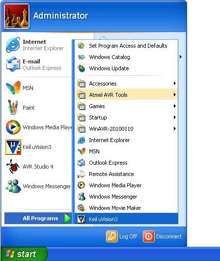
- Step 1: Launch Keil uVision3(click here to download)
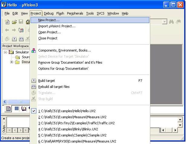
- Step 2: From Keil uVision3 menu bar, select Project > New Project.
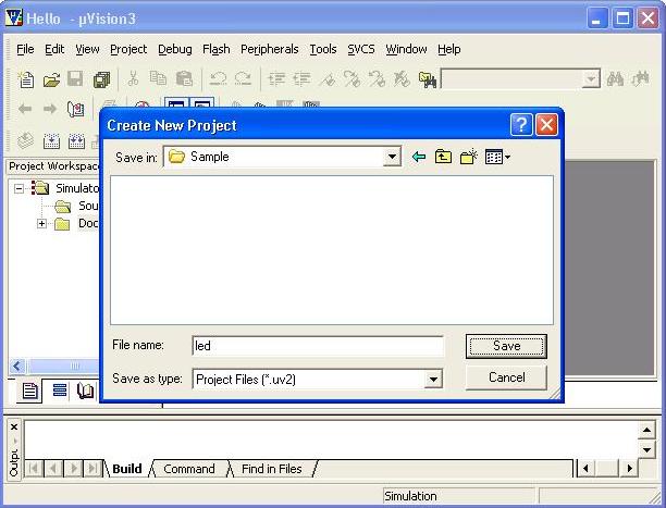
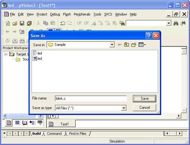
- Step 3: The following window opens. Save the project by providing suitable project name. In the example shown here project is saved by the name ‘led’ as shown in the figure below.
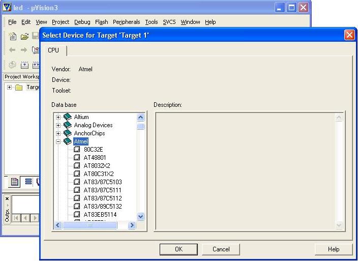
- Step 4: Up on saving the project following window opens. Select the device (AT89S52) to be programmed from the drop down list provided in the window; in the list provided devices are grouped under their manufacturers name (AT89S52 is an ‘Atmel’ make and therefore it can be found under the tag ‘Atmel’ as shown below). After selecting the device click “OK”.
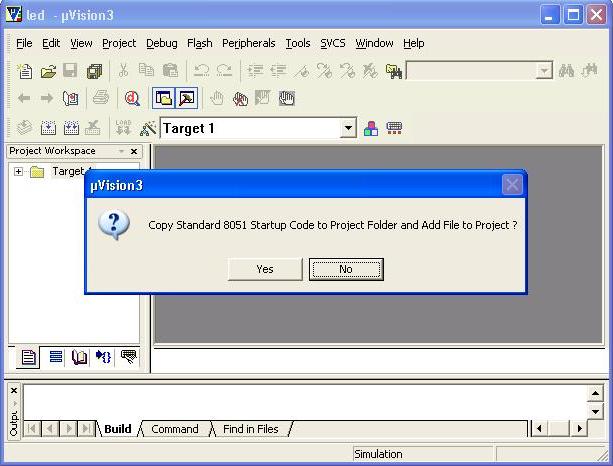
- Step 5: Select whether you need the standard 8051 startup code or not.
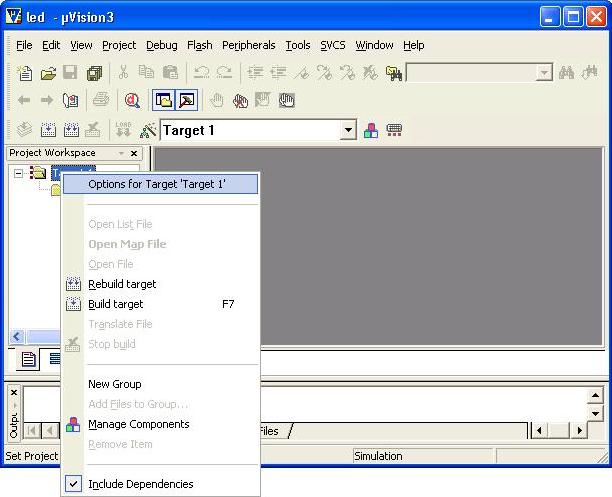
- Step 6: Right click Target 1 and select ‘Options for Target ‘Target 1’’.
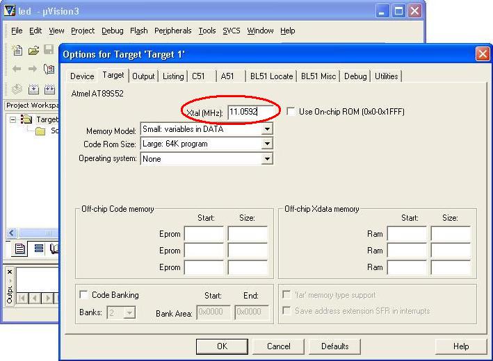
- Step 7: A window opens with options for the target. From the ‘Target’ tab > Select Xtal(Mhz):11.05
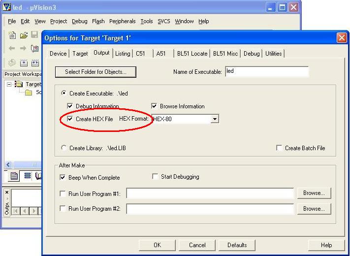
- Step 8: Now on the same window, from the ‘Output’ tab > Make sure the ‘Create HEX File’ box is checked and click OK
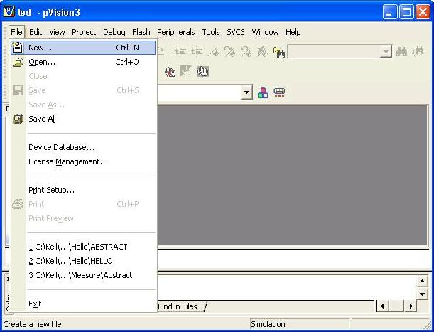
- Step 9: From the main window select the New File icon or select File >New or press Ctrl + N.
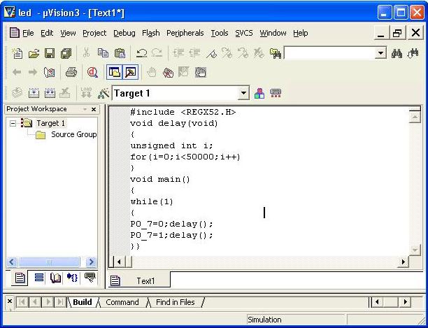
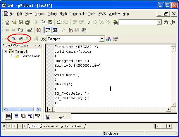
- Step 10: Enter the code to be programmed on to the controller in this new window. Here the code for LED blinking (LED1 connected to fifth pin of PORT1 is shown in the figure as an example.
- Step 11: Now select F\]ile > Save As or press Ctrl + S and save the file using suitable file(blink is the file name used here) name with a .c extension.
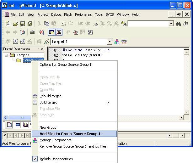
- Step 12: Right click Source Group and select ‘Add Files to Group’.
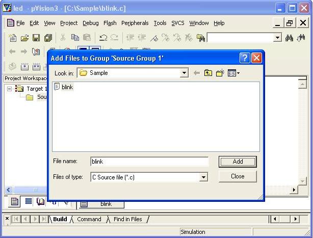
- Step 13: Browse the program file with the .c extension(one that was saved in the previous step). And click ‘Add’ to add the program file to your project (in this example blink.c).
- Step 14: Now build the project by clicking the build option in the main window (build option is marked in red in the figure shown below).
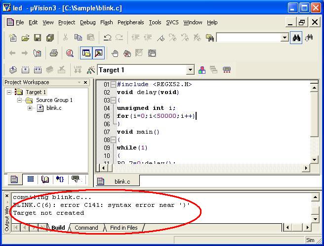
- Step 15: Now on building the project errors and warnings (if any) get listed in the output window. Here in this example a syntax error is illustrated in the figure below (on line number 5; missing semicolon) just to show how the window appears upon an error. Correct the error and build again.
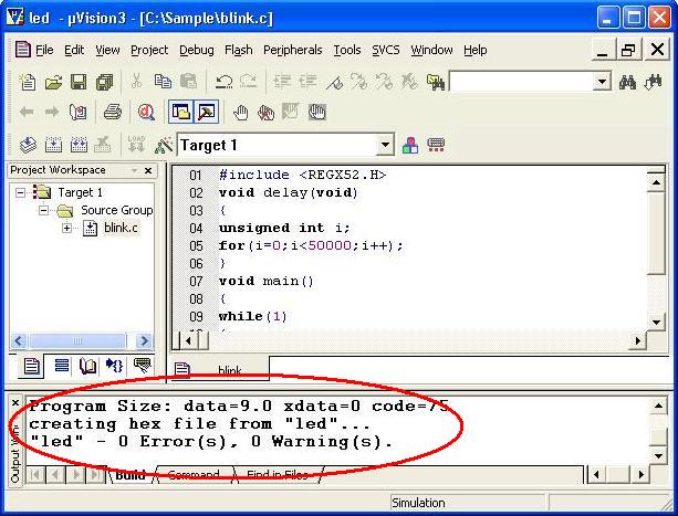
- Step 16: On successful building, the hex file(named after the project) will be generated in the project folder. In the example shown here hex file ‘led.hex‘ will be created in the project folder.
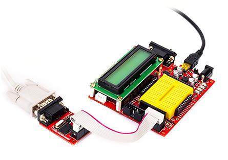
- Step 17: Now to load this program to the controller on the QSB, connect the QSB via ISP to the PC(as shown in the fig below). The rhydoLABZ AT89S52 Quickstart Board is compatible with PHILIPS programmer as well as ATMEL Programmer with on board ISP connector pins for both. In this illustration program is loaded to the controller using the ATMEL Programmer.
 Make sure the programmer, used for loading the program, is connected to correct connector pins provide on board, i.e PHILIPS Programmer to PHILIPS ISP Connector pins and ATMEL Programmer to ATMEL ISP Connector pins respectively.
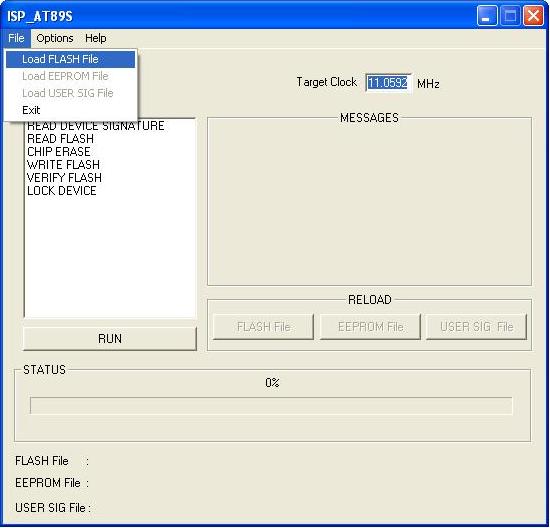
- Step 18: After connecting the Development Board to PC (as shown in the previous step), open the ISP_AT895 application(click here to download). The following window opens. In here select the Target Clock Frequency (11.0592 MHz).
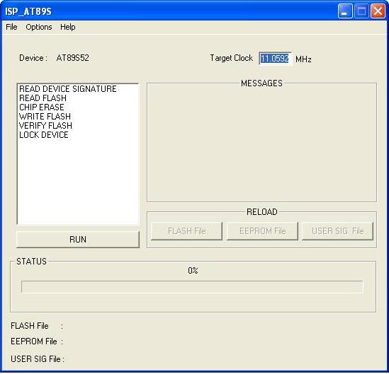
- Step 19: After selecting the target clock frequency select File >Load Flash File and load the .hex file as shown in the next step.
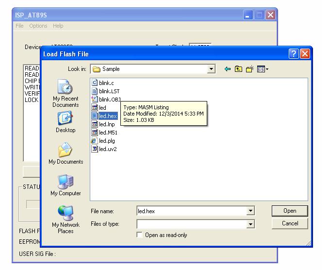
- Step 20: Browse the .hex file (as shown in the figure below) from the project folder.
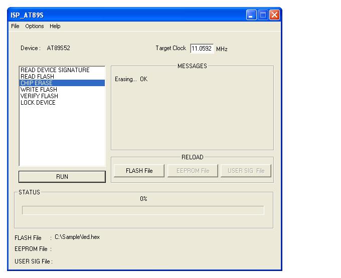
- Step 21: Now select the ‘Chip Erase’ option and run the same to erase any previous loaded program from the chip.
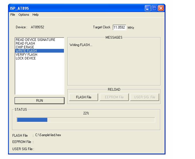
- Step 22: Select the ‘Write Flash’ option and click the Run button to write the program to the chip, status of the writing process will be shown on the bottom of the window.
Topics related to AT89S52 Mini Development Board![]()
- AT89S52 Mini Development Board – Overview
- AT89S52 Mini Development Board – LED Interfacing
- AT89S52 Mini Development Board – LCD Interfacing
- AT89S52 Mini Development Board – Serial communication
- AT89S52 Mini Development Board – EEPROM Interfacing
- AT89S52 Mini Development Board – Buzzer Interfacing
- AT89S52 Mini Development Board – Servo Motor Interfacing
- AT89S52 Mini Development Board – Switch Interfacing
- AT89S52 Mini Development Board – RFID Interfacing
Resources![]()
Shop With Us![]()
- Click here to buy the rhydoLABZ AT89S52 Mni Development Board (Mini) V1.01
- Click here to buy the rhydoLABZ AT89S52 Development Board
- Click here to buy the rhydoLABZ AT89S52-24PU Microcontroller
- Click here to buy the rhydoLABZ ATMEL 89SXX ISP Programmer (RS232)
- Click here to buy the rhydoLABZ Atmel ISP Programmer – USB
Support![]()
Please share your ideas with us, visit our forum for discussion
Leave a Reply
You must be logged in to post a comment.